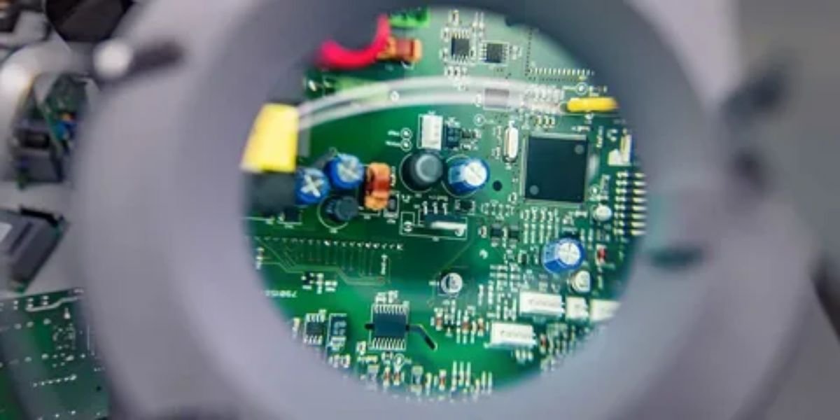
Designing a circuit on glass feels like a significant leap from standard fabrication. A glass PCB simply swaps out the familiar FR-4 epoxy composite for a solid glass substrate. That switch gives you more than just optical transparency; you get superior thermal stability and the kind of low signal loss that high-frequency applications demand.
But glass behaves very differently from the laminates we are used to. It is unforgiving with mechanical stress, and its thermal expansion properties can ruin a design if you aren’t careful. Before you finalize a layout or contact a glass PCB manufacturer, we need to look at the practical realities of the material. We’ll walk through the mechanical limits, thermal behaviors, and specific fabrication strategies you need to ensure your board actually works.
Managing the Fragility of Glass Substrates
Glass is rigid and strong under compression, but it doesn’t forgive mistakes. Unlike standard FR-4, which has enough epoxy and woven fiber to handle a bit of flexing, a glass PCB is brittle. If you push it too far, it doesn’t just bend; it cracks. You need to treat your glass substrate more like a ceramic wafer than a traditional circuit board.
This brittleness means size matters. Large panels are naturally more prone to snapping during assembly simply due to leverage and weight. So, can you fix this at the material level? Many designers now opt for tempered glass—similar to the material protecting your phone screen—which handles impact far better than raw glass. There is also the option of ultra-thin glass. At thicknesses down to 0.1 mm, research suggests these sheets can actually survive drop tests and offer slight flexibility for foldable devices, though they still lack the ruggedness of polyimide.
Designing for Stress Relief
When laying out your board, you have to hunt down stress points. Sharp internal corners or abrupt notches in the board outline act as stress concentrators. Under shock or thermal expansion, cracks inevitably start there.
The fix is to smooth everything out. Use gentle curves and rounded fillets for any cutouts rather than 90-degree angles. Even your copper traces need attention; avoid sudden width changes near connector edges or mounting holes where mechanical strain is highest. A gradual trace transition distributes that stress more evenly.
Fabrication and Handling Tips
Your mounting strategy is just as critical. You can’t just screw a glass board down tightly against metal. We always recommend using plastic washers or spacers to cushion the mounting points and absorb shock.
To keep production yields high, follow these guidelines:
● Choose the Right Cut: Traditional routing puts too much mechanical stress on the edges. Laser cutting is almost always the preferred method for depanelizing glass to prevent edge cracks.
● Communicate with Your Shop: Make sure every operator knows this is glass. Your assembly house should use soft fixtures and avoid any prying or bending motions during rework.
● Check Your Panelization: If you need a large array, work with your glass PCB manufacturer early. They can help you design a panel layout that minimizes stress during transport and automated assembly.
● Add a Buffer: Applying an optically transparent solder mask or conformal coating doesn’t just insulate; it provides a necessary layer of scratch protection.
Calculating Thermal Expansion in High-Heat Environments
When the temperature rises, glass behaves very differently from the FR-4 we are used to. One of the biggest reasons engineers switch to a glass PCB is its incredibly low coefficient of thermal expansion (CTE). In simple terms, it doesn’t warp or stretch much when it gets hot.
To understand why this matters, look at how the materials stack up against copper:
| Material | CTE (Expansion Rate) | The Risk |
|---|---|---|
| Copper | ~17 ppm/°C | Baseline |
| FR-4 | ~14 ppm/°C | Expands significantly; stresses solder joints. |
| Borosilicate Glass | ~3.2 ppm/°C | Stable. Good match for Silicon chips. |
| Quartz / Fused Silica | ~0.5 ppm/°C | Ultra-Stable. Almost zero movement. |
The Real-World Impact
Imagine your device cycling from room temperature up to 150°C. On a 100 mm FR-4 board, that heat could cause an expansion of nearly 0.2 mm. It sounds small, but it’s enough to strain a solder joint to its breaking point.
In contrast, a glass substrate under the same conditions moves only a few micrometers. This stability protects your vias and ensures your board stays flat, which is critical for precision applications in aerospace or automotive sectors.
Strategies for Success
However, lower isn’t always better—you have to look at the whole system. Here is how to manage the thermal mismatch:
● Match the CTE: Don’t just pick the lowest number. If you are mounting silicon chips, a borosilicate glass (~3 ppm/°C) is often a smarter choice than quartz. It moves with the silicon, whereas overly rigid quartz can cause copper traces to shear off.
● Watch the Reflow Profile: Glass hates thermal shock. While most glass PCBs handle lead-free soldering fine, we recommend a gentler ramp-up and cool-down in your oven. Give the glass—and the copper—time to expand and contract together.
● Check the Solder Mask (Tg): Ensure your solder mask’s transition temperature is high enough for the board’s operating range. There is no point in a substrate that survives 300°C if the mask fails at 150°C.
Optimizing Your Layout for Maximum Transparency
Designing on glass is usually about one thing: the aesthetic “wow” factor of a see-through board. But a circuit is never 100% transparent by default—physics gets in the way. You still have opaque copper traces and components to deal with. The goal isn’t invisibility, but discretion. With the right layout choices, we can achieve up to 85% light transmittance, making the circuitry virtually disappear.
Minimize the “Copper Footprint”
Copper blocks light, so your first task is to starve the layout of metal. You need to use the thinnest traces your manufacturer allows. Modern photolithography on glass can achieve line widths down to 50 µm, which is barely visible to the naked eye. If your current limits allow, we also recommend specifying thinner copper foil (e.g., 9 µm instead of the standard 35 µm) to make the traces less prominent.
If you need near-total invisibility—for example, on a display overlay—you might ditch copper entirely for Indium Tin Oxide (ITO). This is the clear conductive material used in touchscreens. Just remember that ITO has higher resistance than copper, so it’s best reserved for low-current signals or capacitive sensing.
Smart Placement and Routing
You have to design with the viewer’s perspective in mind. If the board sits behind a screen, place components on the back side. They will appear as blurred shapes rather than distinct blocks blocking the view. You should also aggressively reduce visual clutter by shrinking your components—swap those 1206 resistors for 0402s or smaller.
Here is a layout trick: On a two-layer board, try to overlap your top and bottom traces. If a signal on the top layer runs directly parallel to one on the bottom, the viewer sees a single line rather than two separate ones. It requires strict constraints in your CAD software, but it significantly lowers the visual density of the circuit.
The Finishing Touches
Don’t let the final manufacturing steps ruin your clear layout.
● Solder Mask: Standard green is obviously out. Specify a transparent solder mask to protect the copper without adding haze.
● Silkscreen: Skip the component markings in the viewing area. Move your reference designators to a hidden board edge or a bezel area.
● Surface Finish: We recommend ENIG. It is less visually intrusive than bright HASL or silver finishes and provides a flat, stable surface for those tiny components.
Overcoming the Challenges of Special Fabrication Methods
Design is only half the battle. Fabricating a glass PCB is where things get tricky. You can’t simply email your Gerbers to a standard board shop and expect a working product. The reality is that glass manufacturing is a niche capability, and only a handful of suppliers worldwide have the right equipment to pull it off.
Why is it so different? For starters, forget about mechanical drilling. If you try to punch a hole through glass with a standard drill bit, the substrate will crack instantly. Instead, manufacturers use precision lasers (often UV or femtosecond lasers) to “ablate” or vaporize tiny holes without stressing the material.
The same goes for cutting the board out of the panel. Mechanical routing—the standard way to cut FR-4—shreds glass edges. Successful fabrication requires non-contact methods like laser cutting or waterjetting. In fact, switching to laser cutting has been shown to reduce edge defects by up to 85%, boosting yields dramatically.
Choosing the Right Partner
Given these specialized steps, you need a manufacturing partner who isn’t just experimenting with glass, but one who has a dedicated line for it. A shop that tries to “swap out” FR-4 for glass on a standard line will likely fail. You need custom vacuum tables, specialized plating chemistries for Through-Glass Vias (TGVs), and operators trained in brittle material handling.
This is where working with an experienced glass PCB manufacturer like Jarnistech becomes invaluable. They don’t just build to print; they provide critical DFM feedback. For instance, they might recommend a minimum glass thickness to ensure the board survives handling or suggest specific pad structures to relieve stress at via entries.


